2.2.4 Sensors
Sensors are the key elements of any IoT solutions, as monitoring the parameters of the surrounding environment starts with physical sensing. The most general definition of a sensor is a device that is acting as an interface between an electronic circuit and the environment The Endrich IoT SBC board has been equipped by several sensors, and also offer the possibility to link external sensors, sensor boards via standard interfaces. The onboard sensors are Everlight’s ambient light sensor (ALS), Tateyama and Semitec temperature sensors (NTC), the magnetic sensor from TDK-Micronas (Hall), Sensolute’s miniature vibration sensor and the MEMS microphone produced by BSE. In this section of the operations manual we discuss the physical background of the sensors’ operation, the way to interface them to the GD32VF103 MCU. In later section we will show how to write the software for the MCU, which calculates the measured environmental data out of the sensed electrical parameter (voltage).
The analogue sensors, which provide an analogue voltage output in the function of the measured environmental parameter are interfaced with the MCU through the A/D converters available. Up to two 12-bit 1MSPS multi-channel ADCs are integrated in the GD32VF103 device. Each is a total of up to 16 multiplexed external channels with 2 internal channels for temperature sensor and voltage reference measurement. An analog watchdog block can be used to detect the channels, which are required to remain within a specific threshold window. A configurable channel management block of analog inputs also can be used to perform conversions in single, continuous, scan or discontinuous mode to support more advanced usages. The ADCs can be triggered from the events generated by the general level 0 timers (TIMERx=1,2,3) and the advanced timers (TIMER0) with internal connection. The internal temperature sensor has to generate a voltage that varies linearly with temperature. The conversion range is between 2.6 V < VDDA < 3.6 V. The temperature sensor is internally connected to the ADC_IN16 input channel which is used to convert the sensor output voltage into a digital value.
The digital sensors are connected through internal inter-integrated circuit (I2C) interface. The I2C interface is an internal circuit allowing communication with an external I2C interface which is an industry standard two-line serial interface used for connection to external hardware. These two serial lines are known as a serial data line (SDA) and a serial clock line (SCL). The I2C module provides transfer rate of up to 100 kHz in standard mode, up to 400 kHz in the fast mode and up to 1 MHz in the fast mode plus. The I2C module also has an arbitration detect function to prevent the situation where more than one master attempts to transmit data to the I2C bus at the same time. A CRC-8 calculator is also provided in I2C interface to perform packet error checking for I2C data.
2.2.4.1 Ambient light sensor
Sensing visible light is important for general lighting, security and other applications. The condition of the proper operation is, that the sensor element has to have a similar response to visible light as the human eye. The conventional device being used in the past was the photoresistor, which however contains dangerous material (Cd-S), making it failed using today due to the strong requirement of RoHs. Standard silicon phototransistors and photodiodes are sensitive for radiation with wavelengths between 400 and 1100 nm. Especially in the infrared range between 800 and 1100nm the sensitivity of silicon devices are quite high compared to the sensitivity in the visible range between 400 and 800 nm. As a consequence such detectors output a relatively high signal under twilight condition, because in this case there is much more infrared radiation present than visible light. This renders the standard silicon photodetectors unusable as (visible) light sensors. Ambient light sensors are optical sensors (photodiodes, phototransistors or photo-ICs) which show a very similar sensitivity spectrum compared to the human eye. This ensures that the signal of the ambient light sensor correlates with the subjective impression of the human eye.
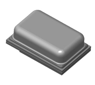
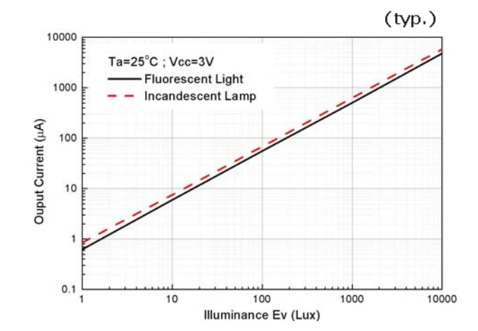
One of these devices is the ALS-PDIC15-21C/L230/TR8 Ambient Light Sensor Device from Everlight, which incorporates a photodiode and a current amplifier IC in a single chip, is a good effective solution to the power saving of display backlighting of mobile appliances, such as the mobile phones and PDAs. Due to the high rejection ratio of infrared radiation, the spectral response of the ambient light sensor is close to human eyes. We placed this sensor to the Endrich IoT SBC Board in order to provide it with the capability of sensing visible light.
Features :
- Close responsively to the human eye spectrum
- Light to Current, analog output
- Good output linearity across wide illumination range
- Low sensitivity variation across various light sources
- Operating temperature performance, -40oC to 85oC
- Wide supply voltage range, 2.5V to 5.5V
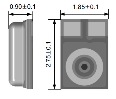
- Size : 3.2mm(L)*1.5mm(W)*1.05mm(H)
- RoHS compliant and Pb Free package
The datasheet of the device can be accessed in the below link or by scanning the QR code on the right:
Interfacing the sensor to the MCU is done by using PA3 ADC input of the GD32VF103 according to the figure below:
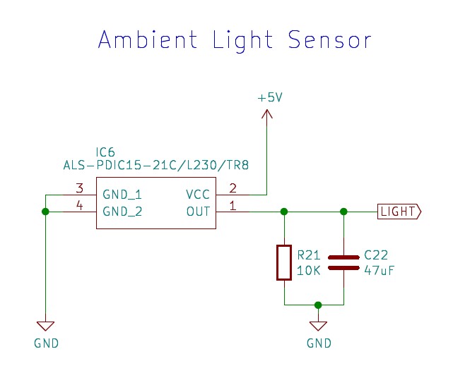
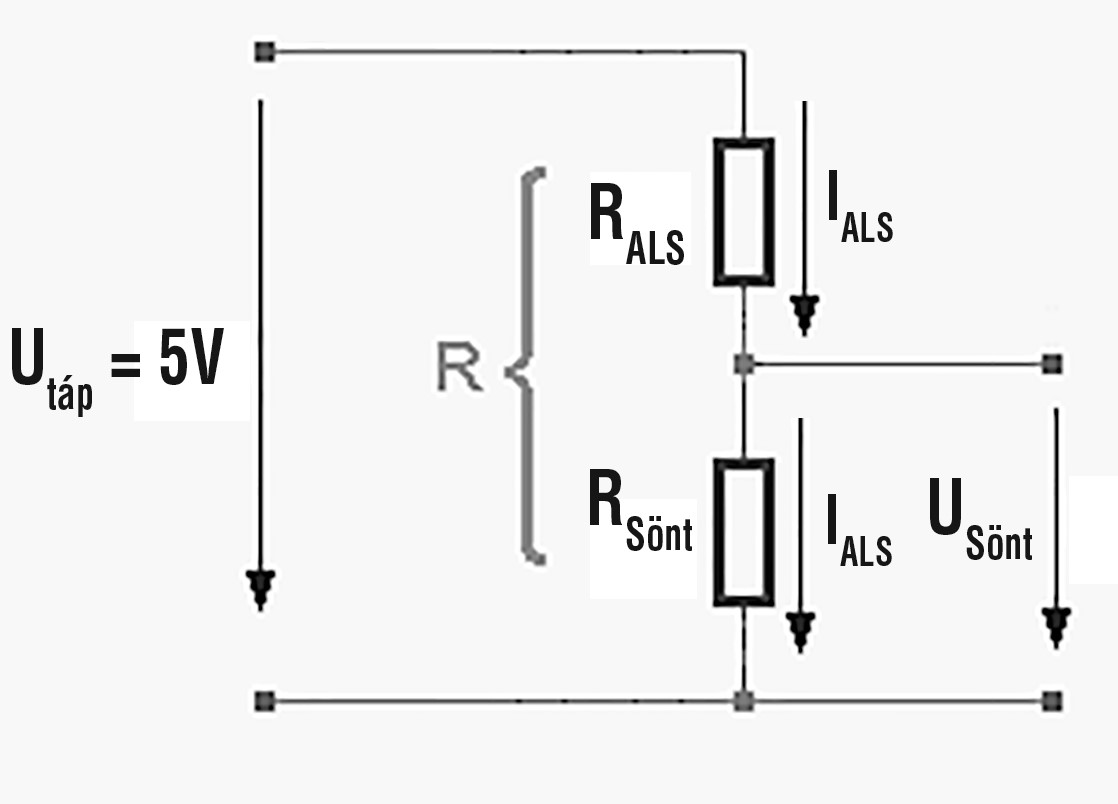
The sum of the voltage drop on the R21 resistor and the voltage drop - proportional to the light intensity - on the internal internal resistance of the ALS sensor result in the supply voltage of 5V. Measuring the voltage drop on R21 by the ADC of the GD32VF103 one can calculate the current of the ALS sensor output. Using the linear correlation between illuminance and current the measured light intensity can be received.
2.2.4.2 Hall effect sensor
Sensing the presence of magnetic field is a common requirement for IoT applications, such as smart meters, where strong magnets are capable to negatively influence the metrology. Most of utility companies require the detection of the presence of magnets, which task can be carried out by using Hall effect sensors. The basis of the operation is the so-called HALL-effect. The electrons of the current flowing in an electrical conductor are diverted from their normal direct path by an external magnetic field perpendicular to their motion. Due to the so-called Lorentz force a potential difference (the Hall voltage) is created, proportional to the field strength of the magnetic field and to the current. Silicon is used almost exclusively as a basic material for the technical implementation of magnetic field sensors as the Hall-effect is most pronounced in semiconductors. In modern Hall-effect sensor devices the magnetic field sensitive Hall element is combined with the signal processing on a single silicon chip.
The simplest application is to use the sensor as a “digital switch“. The magnetic field strength is measured and compared with a fixed threshold level predefined or programmable in the sensor. As soon as this value is exceeded (switching point) the switching state at the output of the sensor changes and the output transistor is switched on or off. Two types of switches are available: 3-wire versions with an open-drain output or 2-wire versions with a current-coded output.
The Endrich IoT SBC Board uses TDK-Micronas HAL 15xy Hall-switch family member produced in CMOS technology as 3-wire device with open-drain output transistor include a temperature-compensated Hall plate with active offset compensation, a comparator, and an output stage. The comparator compares the actual magnetic flux through the Hall plate (Hall voltage) with the fixed reference values (switching points). Accordingly, the output transistor is switched on or off. The active offset compensation leads to constant magnetic characteristics over supply voltage and temperature range. In addition, the magnetic parameters are robust against mechanical stress effects. The sensors are designed for industrial and automotive applications and operate with supply voltages from 2.7 V to 24 V in the junction temperature range from -40 oC up to 170 oC. HAL 15xy is available in a JEDEC TO236-compliant SMD-package 3-lead SOT23.
Features of HAL 15xy:
- SOT23-3L JEDEC TO236-compliant package
- ISO 26262 compliant as ASIL A ready device
- Short-circuit protected open-drain output and thermal shutdown
- Low current consumption of typ. 1.6 mA
- Operates with supply voltages from 2.7 V to 24 V
- Overvoltage protection capability up to 40 V
- Reverse-voltage protected VSUP-pin (18 V)
- High ESD performance of ±8 kV (HBM)
- Diagnostic features: power-on self test
- Sample frequency of 500 kHz, 2 µs output refresh time
- Operates with static and dynamic magnetic fields up to 12 kHz
- High resistance to mechanical stress by active offset compensation
- Constant switching points over a wide supply voltage and temperature range
- Wide junction temperature range from 40 °C to 170 °C
- Built-in temperature coefficient
- Optimized for applications in extreme automotive and industrial environments
- Qualified according to AEC-Q100 test standard for automotive electronics industry to provide high-quality performance
- Robust EMC performance, corresponding to different standards, such as ISO 7637, ISO 16750, IEC 61967, ISO 11452, and ISO 62132
The datasheet of the device can be accessed in the below link or by scanning the QR code on the right:
HAL15xy_Hall-Effect_Switches_with_Open-Drain_Output_in_SOT23_2DSH .pdf
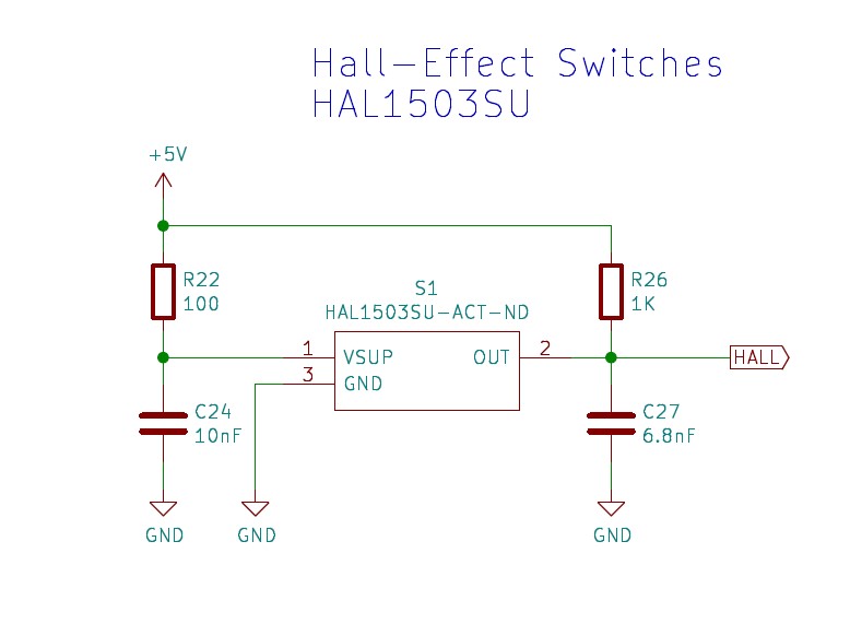
Interfacing the sensor to the MCU is done by using PA4 ADC input of the GD32VF103 according to the figure below:
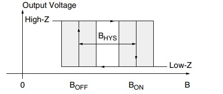
The HAL 1503 unipolar Hall-switch provides high sensitivity. The output turns to Low-Z with the magnetic south pole on the top side of the package and turns to High-Z if the magnetic field is removed. The sensor does not respond to the magnetic north pole on the top side of the package. For correct functioning in the application, the sensor requires only the magnetic south pole on the top side of the package.
Magnetic Features:
- switching type: unipolar
- high sensitivity
- typical BON: 5.5 mT at room temperature
- typical BOFF: 3.7 mT at room temperature
- operates with static magnetic fields and dynamic magnetic fields up to 12 kHz
- typical temperature coefficient of magnetic switching points is -1000 ppm/K at room temperature
Applications:
The HAL 1503 is the optimal sensor for all applications with one magnetic polarity and weak magnetic amplitude at the sensor position, such as:
- clutch position detection
- electric parking brake
- brake light switch
- brake pedal position detection
- steering wheel lock
- door handle
2.2.4.3 Micro vibration sensor
General electronics designs often require a simple device, which is able to detect movement in order to trigger wake-up event for the circuit. A usual way is using ball switches, that are simply but effective components, such as the versions Endrich offers from Sensolute in both uni- and omnidirectional versions.
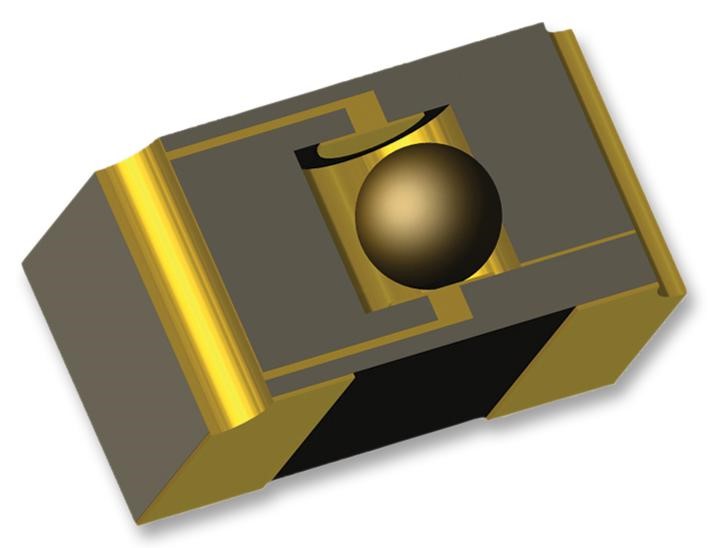
Unlike previously used mercury switches, the micro vibration sensor is environment friendly by using non-toxic substances and therefore it is RoHS and REACH compliant.
The VS1/2 Micro Vibration Sensor detects motion and vibrations through a gold-plated, moving micro-ball encapsulated in a micro barrel, that forms together a ball-switch. Due to its small size of 2,85 x 2,45 x 1,7 mm, the sensor is suitable to use in very small electronic devices by applying SMD technology and can easily be integrated into any designs. The hermetically closed capture makes it resistant against harmful environmental impacts such as humidity or presence of acids, while also having no dangerous substances inside. It could be used in the temperature range of -20°C -+70 °C / -40°C - +85°C and it is fully automatic lead-free SMT mountable.
A micro-ball with a diameter of as small as 0.8mm is located in a cylinder formed by the inner wall of the sensor housing and can move freely inside this cavity. Even the smallest movement or vibration causes the ball to move so that closes or opens two gold-plated contacts, one as the sidewall of the hollow and the other on the bottom of the sensor. The pulses resulting from this vibration should be evaluated by application-specific electronics and are implemented in corresponding switching signals. As soon as the sensor detects no more movement, the electronics could switch to the power-down mode after an application-specific time delay. This seems very easy, and theoretically could be easily implemented and used to switch off electrical devices such as handheld devices being not in use, vehicle electronics, that should not be used when standby, or shut down control circuits of machines, that are switched off, all for saving battery lifetime and power consumption.
As the sensor does not provide a definite „on” state when vibration occurs and „off” state at rest, we need to implement an electronics, which can evaluate the environmental circumstances. The output of this ball-switch device will be a series of transitions between the logical high and low DC levels. Moreover this both versions of the sensors are not necessary closed when no vibration detected. The unidirectional version is equipped with contacts on one side resulting different sensitivity depending on sensor orientation. This sensor is suitable for motion and position detection. The omnidirectional version is independent of the sensor orientation. This sensor is suitable for motion-detection only. Being at one DC-level a slight vibration may cause the sensor signal to toggle, that cannot be easily filtered out therefore has to be handled by the MCU software. With the unidirectional VS1 sensor it is possible to get a defined open state by building it upside down, as the micro sphere is on the top of the cavity, where is no contact pad present.
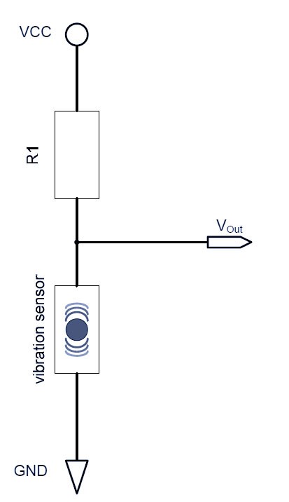
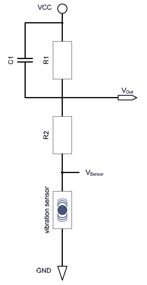
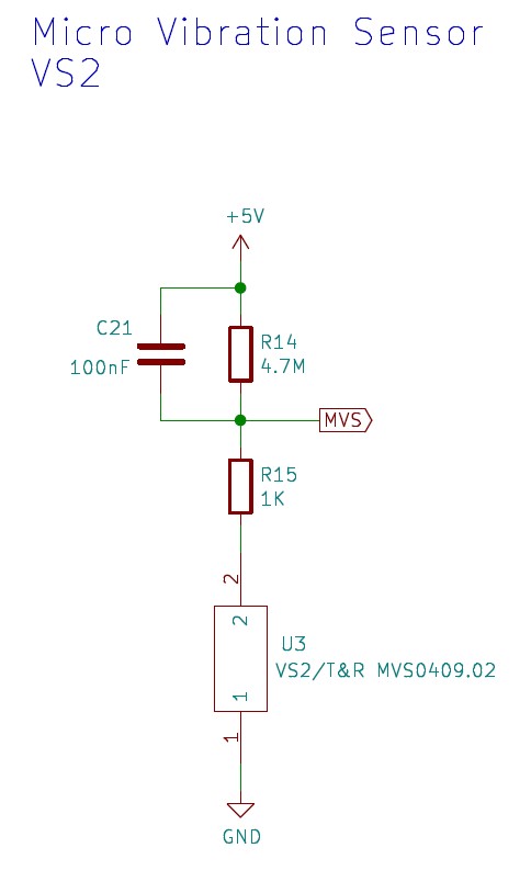
On the left figure (up) the simplest circuit is shown, where the resistor is necessary to limit the current to a maximum value of 2 mA. If the sensitivity of the device should be reduced, a small capacitor could be used in parallel with the resistor. In this case is better to make a voltage divider, by means of using two serial resistors, because if the capacitor is directly on the input of the sensor, the large inrush current could damage the contacts. Therefor a solution shown in the right figure is better. In case using higher capacitance, the peaks of the output voltage will be integrated into an average analog value. For the resistive divider R1=5M and R2=100k .. 1M could be chosen.
In case a definite „low” state is required, when the sensor does not detect vibration, a similar circuit to the one shown of the figure could be used.
The capacitive voltage divider determines the filter characteristics, C2 should be at least 5 times larger capacitance than C1. The C1 value of 100pF will result high sensitivity, while the 100nF value would turn the peaks of the output into an integrated average voltage.
The datasheet of the device can be accessed in the below link or by scanning the QR code on the right:
MVS0409_02-Datasheet%20Rev2_6.pdf
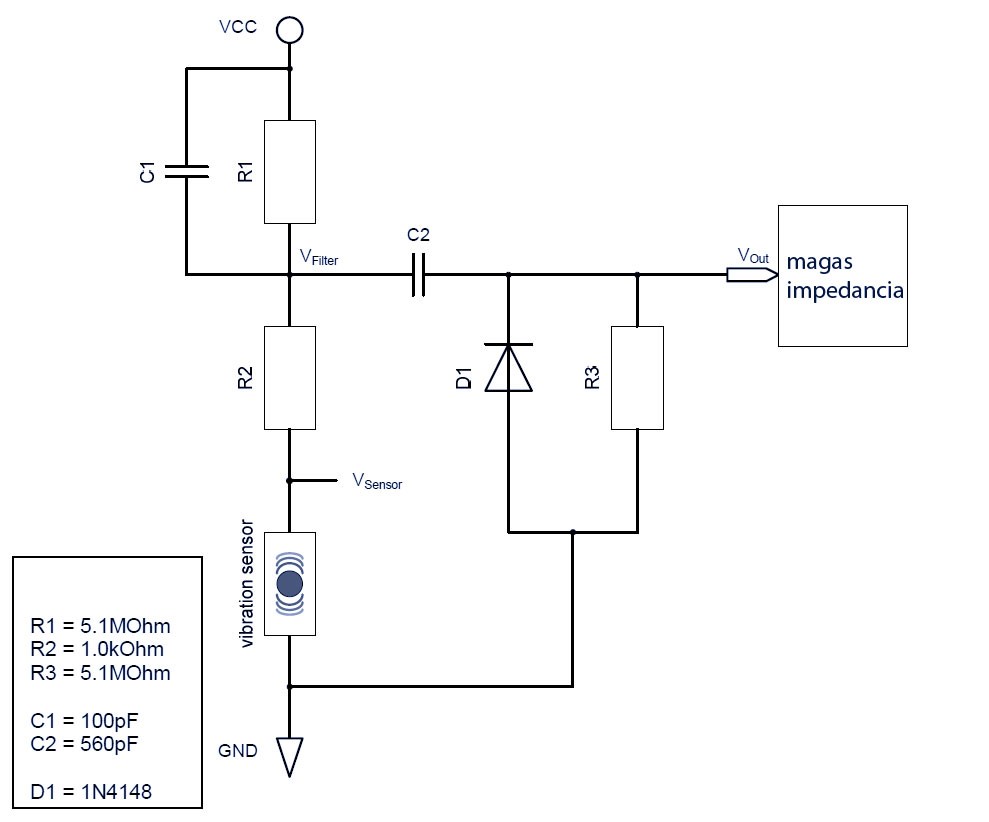
Interfacing the sensor to the MCU is done by using PA5 ADC input of the GD32VF103 according to the figure below:
2.2.4.4 Micro altimeter module
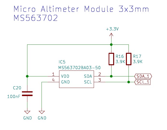
One of the digital sensors used in the Endrich IoT concept has been also placed on the IoT SBC Board. This is the MS5637 low voltage barometric pressure sensor from TE, which has an I2C interface and connected to the GD32VF103 MCU through the MCU’s second I2C channel, SDA_1 and SCL_1 (PB10, PB11), which is used for in-board connection. (MCU’s SDA and SCL have been used for external I2C interface) The MS5637 is an ultra-compact micro altimeter. It is optimized for altimeter and barometer applications in Smart-phones and Tablet PCs. The altitude resolution at sea level is 13 cm of air. So it is also usable to detect steps taken when climbing on stairs indoor. The sensor module includes a high-linearity pressure sensor , temperature sensor (NTC) and an ultra-low power 24 bit ΔΣ ADC with internal factory-calibrated coefficients. It provides a precise digital 24-bit pressure and temperature value and different operation modes that allow the user to optimize for conversion speed and current consumption. A high-resolution temperature output allows the implementation of an altimeter/thermometer function without any additional sensor. The I2C communication protocol is simple, without the need of programming internal registers in the device. Small dimensions of 3 x 3 x 0.9 mm3 allow the integration in mobile devices. This new sensor module generation is based on leading MEMS technology and latest benefits from MEAS Switzerland proven experience and know-how in high volume manufacturing of altimeter modules, which has been widely used for over a decade. The sensing principle employed leads to very low hysteresis and high stability of both pressure and temperature signal. The datasheet of the device can be accessed in the below link or by scanning the QR code on the right:
Interfacing the sensor to the MCU is done by using PB10/11 I2C interface of the GD32VF103 according to the figure below:
2.2.4.5 Temperature sensor
Temperature measurement is one of the most important disciplines in sensor technology. Basically there are contactless and touch-contact measurement methods.
About temperature sensing in nutshell:
The most common and important sensor elements for temperature measurement are the temperature-dependent resistors. Working principle of resistive temperature sensor devices is the dependency of the electrical resistance of a material on its temperature changes. Two main types of resistive temperature sensors are the metallic devices (mainly called resistance temperature detectors), and semi conductive temperature sensors (generally called thermistors).
The first group is characterized by resistance rising with temperature increasing, having positive temperature coefficients (PTC), and unlike the semi conductive thermistor type, their output is extremely linear producing very accurate measurements of temperature. These sensors are made of high-purity conducting metals such as platinum, copper or nickel.
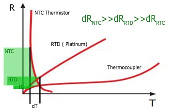
Main disadvantage of RTDs is, that they have very poor thermal sensitivity, meaning a change in temperature only produces a very small resistance change like, 1r/°C (see figure). The most common types of RTD’s are made from platinum and are called Platinum Resistance Thermometer or PRT‘ s, like the PT1 00 sensor, which has a standard resistance value of 1 00r at 0°C. The main disadvantage of this type of device is the cost, platinum is an expensive material. A typical RTD has a base resistance of about 1 00r at 0oC, increasing to about 1 40r at 1 00°C through the operating temperature range of -200 to +600°C. As measuring temperature needs to involve sensing the voltage drop on the device, we need to pass a current through the resistor. Any variation in resistance due to I2R self-heating causes an error in the readings. To avoid this, the RTD is usually connected into a Whetstone Bridge network.
Thermistors
The second group of resistive temperature sensors is the thermistor devices. Their working principle is based on non-linear resistance change in a ceramic semiconductor material with temperature rise. They are either NTCs (Negative Temperature Coefficient), which conduct the electrical current at high temperatures better than at low temperatures, or PTCs, with reverse behavior. As seen on the figure, unlike NTCs, PTCs usually have linear R-T characteristic, the advantage of the NTCs is however the better sensitivity: for the same change in temperature, the resistance change response is much more robust than with PTC or thermocouple.
The second group of resistive temperature sensors is the thermistor devices. Their working principle is based on non-linear resistance change in a ceramic semiconductor material with temperature rise. They are either NTCs (Negative Temperature Coefficient), which conduct the electrical current at high temperatures better than at low temperatures, or PTCs, with reverse behavior. As seen on the figure, unlike NTCs, PTCs usually have linear R-T characteristic, the advantage of the NTCs is however the better sensitivity: for the same change in temperature, the resistance change response is much more robust than with PTC or thermocouple.
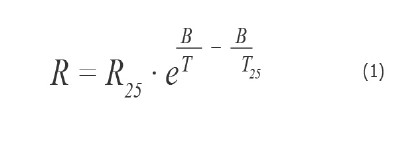
T25 = 298,15 K (25°C), T: temperature in K
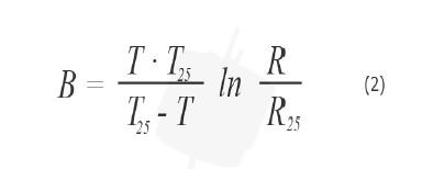
R25 indicates the value of the resistance at the reference temperature of +25°C the so-called B-value (in Kelvin K) describes the behavior between resistance and temperature and determined by the following logarithmic expression:
For most applications (1) provides a sufficient mathematical correlation between resistance and temperature over a wide temperature range of 0°C -1 00°C with the accuracy of ±1 °C.
Should a higher accuracy be required, we need to use the best known approximation between resistance and temperature, the so called Steinhart-Hart equation:
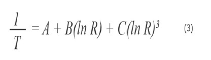
The R determines the resistance value on temperature T in (3), A, B and C are the so called Steinhart-Hart coefficients, that are derived from experimental measurements. These coefficients can be requested from the supplier of the thermistor element. This formula provides ±0.1 5°C accuracy in the temperature range of -50°C to +1 50°C, what is usually exact enough for most of the applications. By reducing the temperature range to 0°C to +1 00°C, the accuracy can be increased up to ±0.01 °C.
When designing-in an NTC temperature sensor, the driving current should be set as small as possible in order to avoid the nonlinearity caused by the I2R self heating of the sensor element. The datasheet of the supplier contains the dissipation factor, which indicates the electrical power required to heat up the thermistor by 1 °C over the ambient temperature. In practice it is recommended to stay under this threshold. Finally the NTCs has a certain thermal inertia to consider, therefore to follow temperature change by resistance change requires time. The thermal time constant „t” is defined by the elapsed time till resistance reaches 63.2% of the final value. To achieve customer and application specific requirement of characteristics is always more complex task. Therefor it is crucial that the NTC manufacturer is flexible enough to give fast response to even frequently altering customer requirements. An own research and development department, and the in-house production of NTC chips is therefore mandatory for successful customer specific component design. The R25 and B values are obtained by the mixture and the added nanoparticles before the sintering process. In the Dicing-Process (separation), the wafers are separated into chips (dies) and calibrated for the further production process. The precision below ± 0.05% can be achieved in this way, without the need of selection.
Interfacing thermistor to any MCU
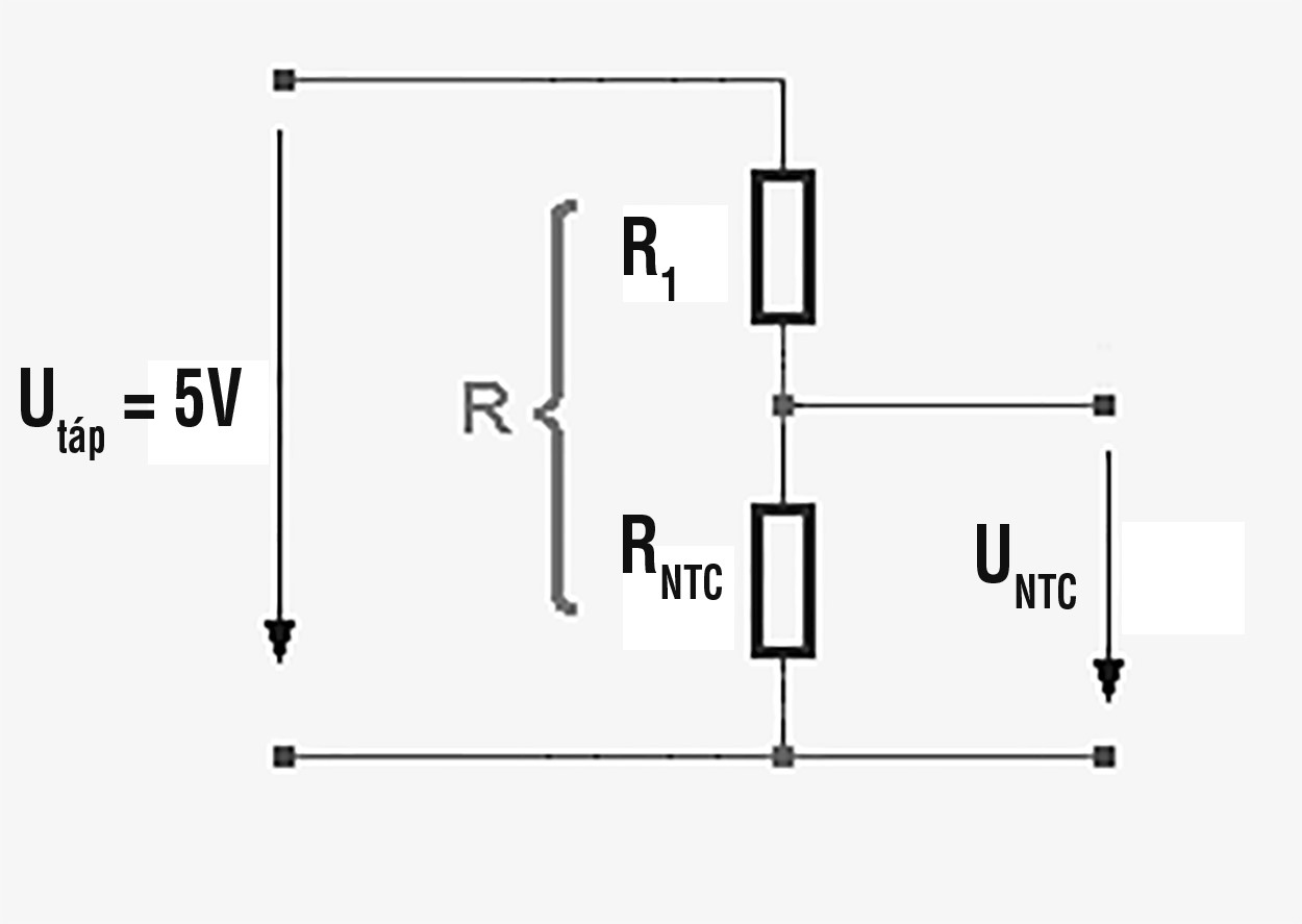
The temperature can be calculated from indirect measurement of the NTC’s resistance. To perform this the MCU needs to measure the voltage drop on the NTC’s internal resistance, and knowing the current of the NTC one can calculate the resistance and out of it the temperature.
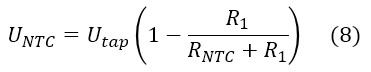
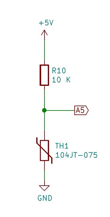
The theoretical schematics on the below figure shows the resistive voltage divider consisting or R1 know serial resistance (practically the same value may be selected as the NTS’s resistance on 25°C), and the RNTC, the resistance of the NTC on the temperature we need to detect. R1 is pulled up to the MCU’s supply voltage.
The common current flowing through the NTC comes from the Ohm rule, INTC = Usupply / (R1+RNTC)
The RNTC resistance can be calculated according to equation (4):
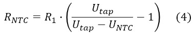
Where R1 and Usupply are known values, and UNTC is the voltage drop measured by the ADC of the MCU.
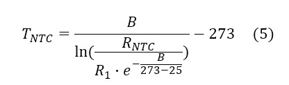
As soon as the RNTC calculated value is in our hand, there are several methods to calculate the temperature
1st method:
For most applications (1) provides a sufficient mathematical correlation between resistance and temperature over a wide temperature range of 0°C -100°C with the accuracy of ±1 °C. (5)
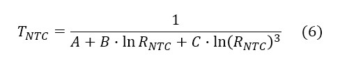
2nd> method:
Should a higher accuracy be required, we need to use the best known approximation between resistance and temperature, the so called Steinhart-Hart equation. The temperature in [°K] can be calculated according to (6):
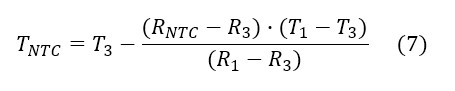
3rd method:
In most of the NTC manufacturer catalogues the R-T table of the element is included or could be requested for the sensor at the producer. The neighboring data pairs are so closed to each other, that the change of resistance in the function of temperature could be supposed being in linear correlation. For one given RNTC value the closest neighboring R1-T1 and R3-T3 data pairs make it possible to calculate the actual temperature of the NTC (TNTC [°C]) according to (7):
The schematics of the real application’s voltage divider can be seen on the picture on the left. As the pull up voltage we can select any of the fixed, known DC voltages available at one of the power supply domains in the system. It is advised to select its and R1’s value on the way, that we could use the whole resolution of the MCU’s ADC. A 12bit ADC divides the whole range of possible NTC voltages into 212 segments, 0 will be rendered to 0V and 4096 to Vcc. At Vcc=5V this resolution will be 0,00122V. If the value of R1 is selected to be same as the NTC’s R25, then the measured voltage at 25°C will be the half of the Vcc (8)
In case RNTC >> R1 (at very low temperatures) the UNTC approximates the Vcc, and on high temperatures, where RNTC << R1, UNTC is nearly zero. We used the whole resolution of the ADC in the range of 0-Vcc:
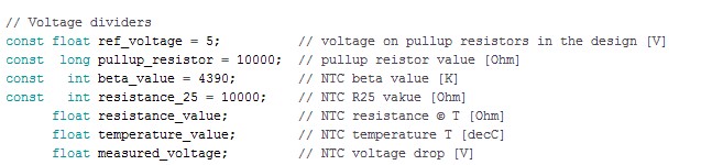
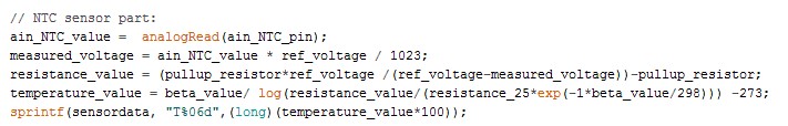
Using the simplest equation (1), the temperature of the NTC can be calculated according to the below sample C code.:
Extremely high accuracy
In those applications, which require high accuracy, the long-term stability of the sensor is important. The initially low tolerance and thus a small measurement error is obvious requirement, but what happens if the resistance value drifts away over time? Main cause of this drift is the moisture that penetrates into the ceramic component. This negative affect can be prevented by glass passivation. The thick-film SMD thermistors of our Japanese manufacturer Tateyama are built on a ceramic substrate (96% Al2O3), and the thick film is provided with a glass cover protected against moisture (see image).
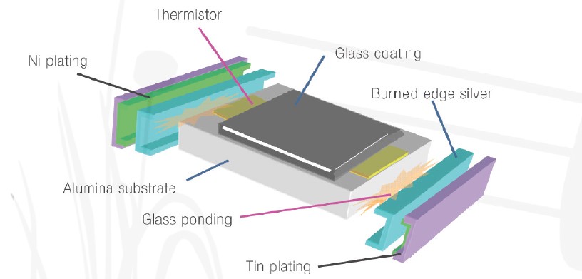
This results in a high mechanical strength against heat expansion, therefore extremely good solderability and reliability. Due to the applied glass layer it is resistive against highly corrosive gases, like e.g. sulfur as well as against moisture. The further advantage of these thick film sensors lays in the variable adjustment of the R25 – (100R to 2M) and B values (2700 – 5000 K) as well as in the corresponding tolerances (± 1 to ± 10 %), which is possible due to Tateyama's patented manufacturing technology. All these SMD thermistors are certified according to TS1 6949 / AEC-Q and available in the sizes of 0805 up to 0201 . Because of the price level and long-term stability, these thermistors can be used in applications such as climate control, heat cost allocators, white goods or power tools. The thick film technology can be used at temperatures up to 150°C. Smaller the form factor, the smaller is the thermal mass and thus the thermal time constant „q”. In applications where the temperature changes quickly, designer is recommended to use the smallest available device, typically the 0201 model. The NTC series from our other Japanese manufacturer Semitec are not based on the thick film, but on ceramic semiconductor technology. They are characterized by small tolerance (± 1 % in B value and R25). The sensor family with the smallest tolerance is the "AP" series (± 0.5 % in B value and R25), at temperature range of -50 to +70 °C, making possible to perform temperature measurements with an accuracy better than 0.5 K without calibration of the system. The thin "KaptonFilm" – NTCs with a thickness of only 0.5 mm are mainly used in rechargeable batteries. The "KT" family is the SMD series thermistor of Semitec. Despite its low pricing, the KT has a very good long-term stability due to the glass passivation on the surface of the ceramic chip that is required for today's electronic heat cost allocators, which are expected ten years of operation without recalibration. The "AT-4" series is widely used in handheld tools, especially the 6.8 kOhm type is suggested to be used in the temperature monitoring electronic of the battery charger circuit.
On the Endrich IoT SBC Board v052 we have not used any of above thermistors, as the micro altimeter device has one inside, as well as the internal temperature sensor of the GD32VF103 MCU provides temperature information of the MCU itself. However, there are Tateyama and Semitec NTCs placed on the external sensor boards, exhibition demos and other Endrich IoT family member hardware elements. Therefor we see to be important to have the detailed discussion of the temperature sensing technology.
2.2.4.6 Analog MEMS microphone
We wanted to have voice analysis possibility on the board in order to offer services as identification of unique sounds such as glass breaking or chainsaw noise. These samples could be used to detect intrusion in home environment or legal woodworking in a forest. A microphone would also be good to sample the volume of background noise as an environmental parameter. In order to sample, first the noise has to be detected, later a Fast Fourier Transformation (FFT) makes it possible to analyze the noise by comparing the major frequencies with some pre-stored samples (frequency). The background noise level can be calculated out of the measured sound pressure level (amplitude).
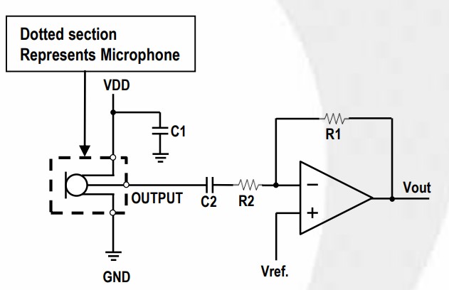
For the detection we have designed in an analogue MEMS microphone. MEMS microphones contains two semiconductor chips in a single package. One of them is a MEMS (micro-electro-mechanic system) membrane which converts sound waves into an electrical signal, while the second circuit is an amplifier. When we talk about digital MEMS, an analog/digital converter (ADC) takes place as well inside the package. Without the ADC a pre-amplified analog output signal is available to the user, this is the way as the bult-in BSE F4-(S)MOE-N090R38-3P microphone is constructed. MEMS microphones with analog outputs should be interfaced to the host circuit through an external operation amplifier. The analog output signal of the microphone is driven by an amplifier inside the microphone offering a reasonable signal level with a low output impedance.
The dc blocking capacitor (C2) is used for eliminating the necessity to match the dc input voltage of the host circuit to the dc output voltage of the MEMS microphone. The pole frequency created by the combination of C2 and R2 needs to be set low enough such that the desired audio frequency signals are passed to the host circuit with an acceptable level of attenuation [i.e. for minimum audio frequency of the microphones’s frequency response curve of 50 Hz; 1/(2*π*R23*C25)< 50 Hz]. Below you can see the theoretical schematics of the microphone interface. The amplified output voltage is connected to the ADC of the microcontroller unit for sampling.
The gain of the amplifier can be set by the proportion of R1 and R2, GAIN = -R1/R2. You can see the real application schematics on the following figure:
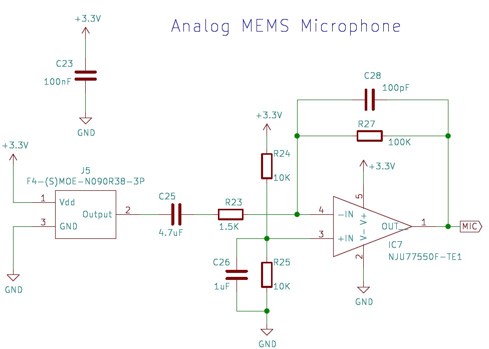
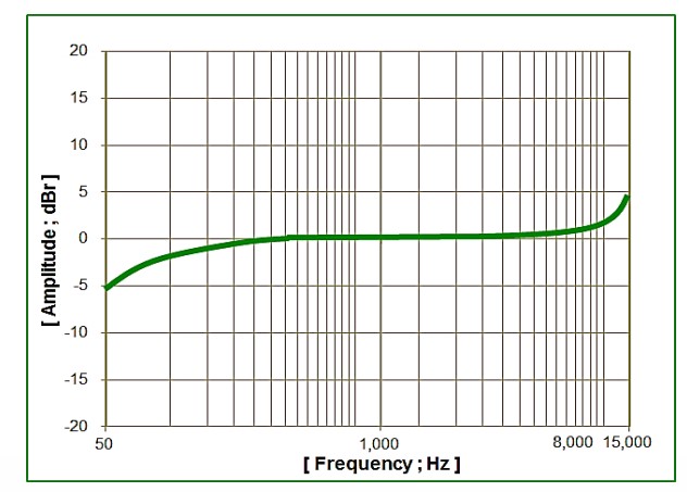
In our case C25 = 4.7uF and R23=1.5k therefore 1/(2*π*R23*C25)< 50 Hz is fulfilled. The frequency response curve of the microphone can be seen here:
The datasheet of the device can be accessed in the below link or by scanning the QR code on the right:
200403_F4-(S)MOE-N090R38-3P_Analog_MEMS_MIC_Specification_V1-0.pdf