2.2 Hardware
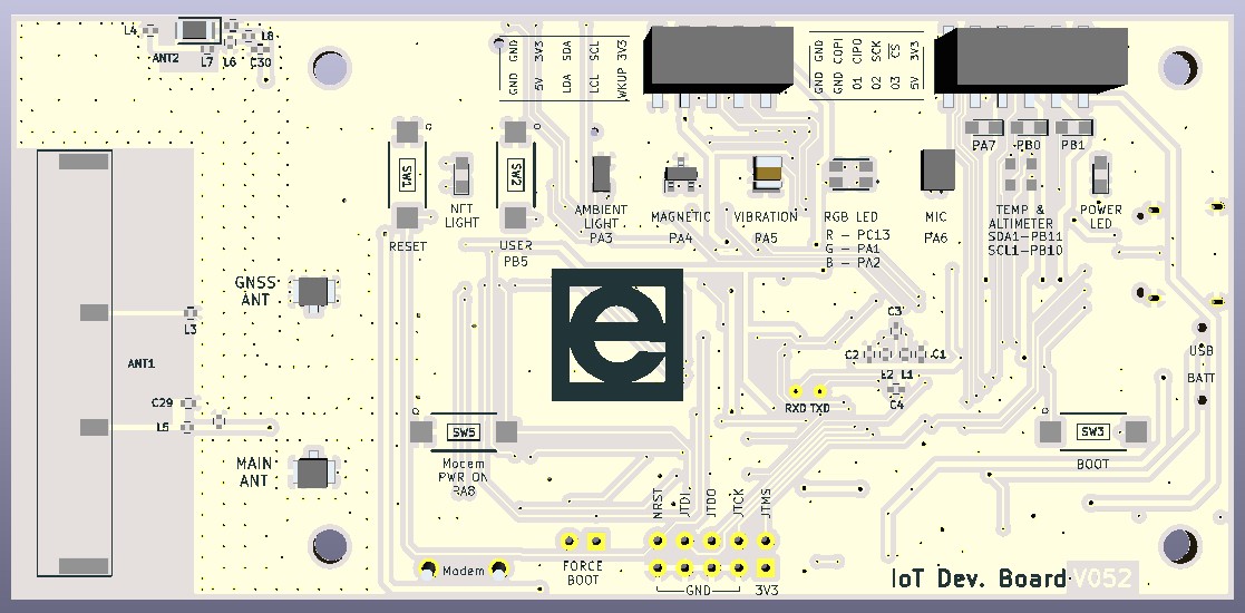
This section contains the complete hardware layout of the Endrich IoT Board (v052) single board computer / evaluation board. The actual (updated) document can be downloaded at any time from schematicsEIBv052.zip address, or through the following QRCode. You can get access to the Gerber files of the PCB as well as all the documents required for mass production, e.g. bill of material, datasheets and position files.

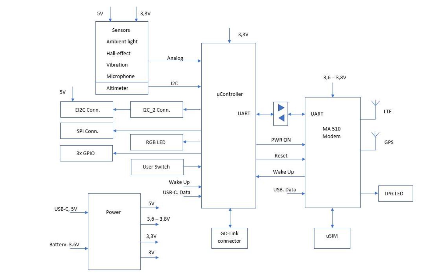
2.2.1 Block diagram of the IoT SBC evaluation board v052
The operation and the hardware capabilities of this IoT Single Board Computer can be best checked on the below block diagram.
You can see the main parts of the hardware, the sensor functions, the power supply segment, the interfaces, the microcontroller and the communication part. The analog sensors are interfaced with the A/D converter inputs of the MCU, while the onboard digital sensors are chained to the MCU’s I2C interface. The power supply segment takes care of the right voltage levels by using DC/DC converters, wherever it needs to boost (in case of 3.6V battery power) or have a buck conversion (when powered by 5V USB). The microcontroller offers I2C and SPI interfaces to the outside world, and features 3 free GPIO (general purpose input output lines) to control external devices such as PWM controllable fans, relay boards, 1-10V light control for special LED drivers. The MCU and the GSM modem are connected via UART interface.
2.2.2 Power supply
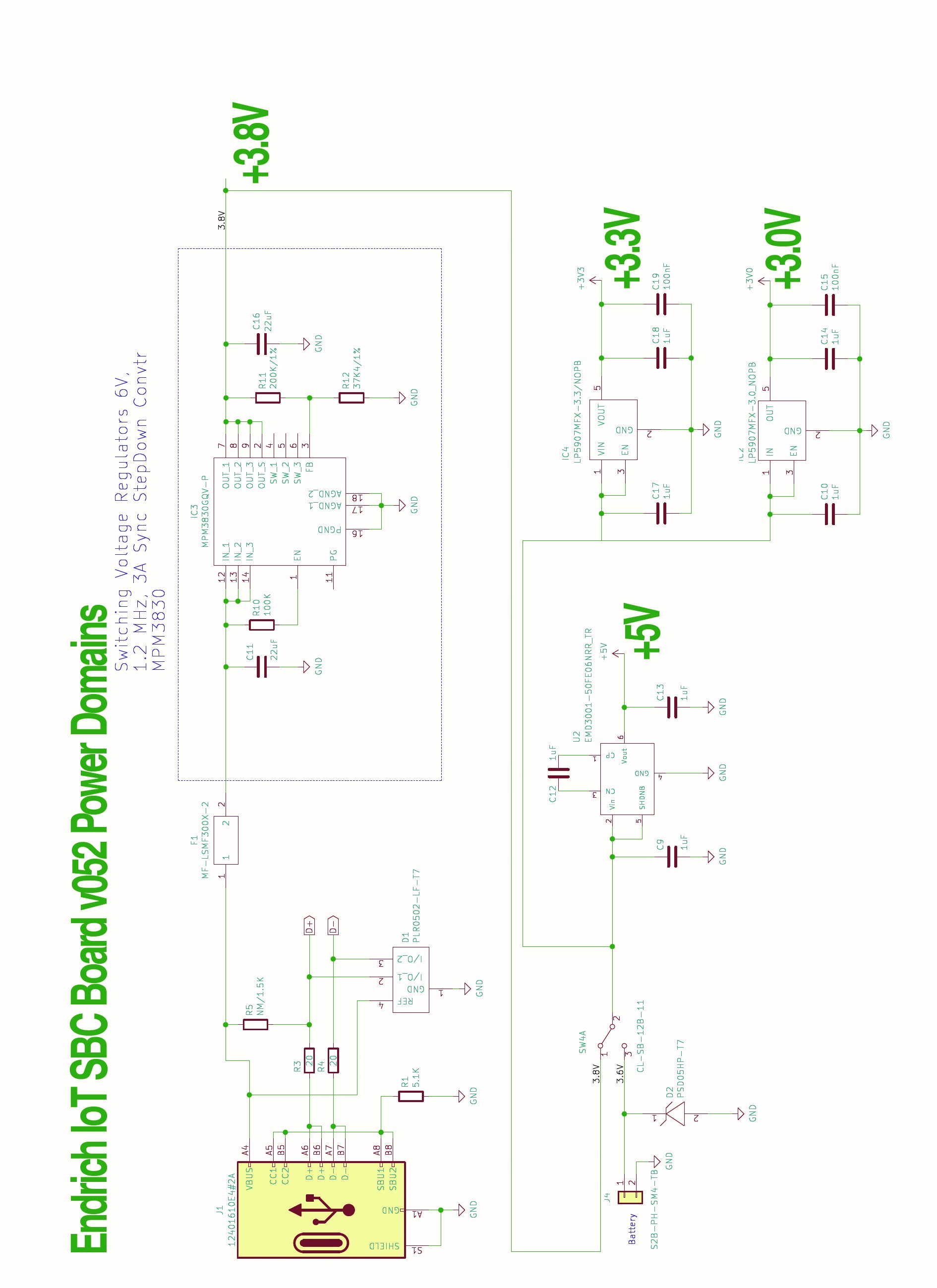
The circuits need several voltage levels, with different peak current handling capabilities. The sensors require 3.3V and 5V, the MCU needs 3.3V and the modem requires 3.8V. All these different voltage levels have to be created from the available power source, what can be a 3.6V primary ER battery cell/pack or USB (5V). The input voltage is selectable by a switch. Switching mode DC/DC step-up and step-down converters offer solution to create these variety of voltages.
You can read about DC-DC converter technology in details at the following link, the author is the head of the design team of the Endrich IoT SBC board.
DC-DC switching power supply regulators from New Japan Radio
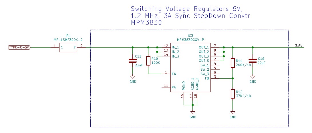
The fist task to solve is to provide power for the GSM modem (3.8V) in case the input is USB power (5V). For that purpose – as the maximum required current is 3A (at requesting connection to tower in GPRS mode) – we have used Monolithic Power System’s minimodule MPM3830.
The MPM3830 is a step-down module converter with built-in power MOSFETs and inductor. The DC-DC module comes in a small surface-mount QFN-20(3mm x 5mm x 1.6mm) package and achieves 3A continuous output current from a 2.7V to 6V input voltage with excellent load and line regulation. The MPM3830 is ideal for powering portable equipment that runs from a single cell LithiumIon (Li+) Battery. The output voltage is regulated as low as 0.6V. We only needed 3.8V with this high constant current, so we used it when the board is powered from USB. Only FB resistors and input and output capacitors were needed to complete the design.The Constant-on-time control (COT) scheme provides fast transient response, high light-load efficiency and easy loop stabilization. Fault condition protection includes cycle-by-cycle current limit and thermal shutdown (TSD).The MPM3830 requires a minimum number of readily available standard external components and is available in an ultra-small QFN20 (3mmx5mm) package. Its datasheet can be downloaded from the below web link, or by using the QR Code on the right side.
The schematics :
The second voltage level , which is necessary for pulling up the analog sensors to is the 5V. For that we needed to perform a step up conversion when using an ER Lithium primary battery ( 3.6V). the chosen DC-DC converter is ESMT’s EMD3001 low noise, regulated charge pump IC. Its two times charge pump and constant switching frequency configuration with low noise characteristics, low external components makes the EMD3001 unique performance and perfect for this portable application. Fixed regulated output voltage (EMD3001) is available for different applications with input voltage range from 2.7V to 4.5V and provide up to 100mA of output current, which is more than enough for the purpose we intend to use it. Soft-start circuitry, preventing the inrush current, thermal shutdown and short circuit protection are all built-in as well. It also features with <1uA low showdown current when the device is disabled. The EMD3001 is available in a 6-pin SOT-26 and TDFN-2x2- 6 package (fixed 5V output). Its datasheet can be downloaded from the below web link, or by using the QR Code on the right side.
The schematics :
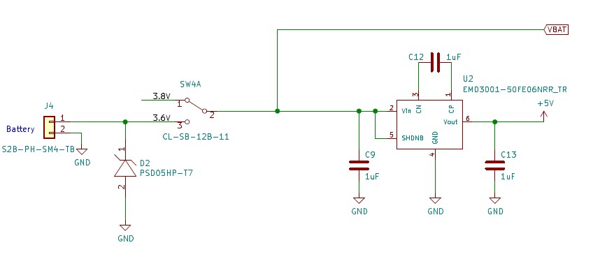
The battery connector is protected against ESD,EFT and Surge by Protek Devices’ PSD05HP transient voltage suppressor diode. The PSDxxHP series are single line, 1000 Watt transient voltage suppression devices designed for use in battery packs to protect sensitive electronics from transients. Available in a SOD-323 package configuration, the PSDxxHP series provide ESD and EOS protection while saving space on the printed circuit board. Other applications for this series include wireless telecommunication devices and portable electronics like SMART phones.
The PSDxxHP series is ideally suited to protect data I/O ports against ESD, EOS and EFT. These devcies exceed the requirements of IEC 61000-4-2 (ESD) and IEC 61000-4-4 (EFT). The PSDxxHP series, in conjunction with passive components integrated into a TVS/Filter network can be used for EMI/RFI protection. Its datasheet can be downloaded from the below web link, or by using the QR Code on the right side.
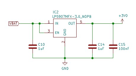
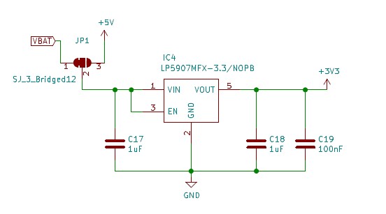
For the 3V and 3.3V we need to drop voltage down from ER battery (3.6V) as well as from USB (5V) power source. As the currents required are relative small, we are fine to use LDOs instead of switching regulators (DC-DC).
2.2.3 Microcontroller (GigaDevice GD32VF103CBT6 RISC-V)
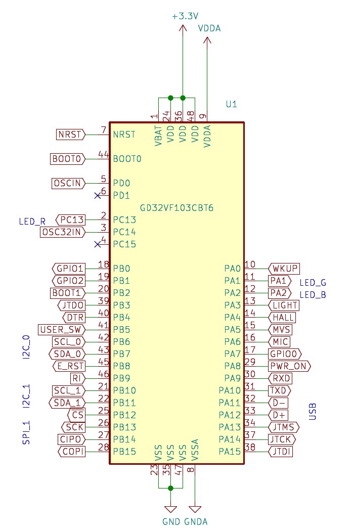
The heart of the Endrich IoT SBC board is the GD32VF103 device of GigaDevice, which is a 32-bit general-purpose microcontroller based on the RISC-V core with an impressive balance of processing power, reduced power consumption and peripheral set.
The GD32VF103 device incorporates the RISC-V 32-bit processor core operating at 108 MHz frequency with Flash accesses zero wait states to obtain maximum efficiency. It provides up to 128 KB on-chip Flash memory and 32 KB SRAM memory. An extensive range of enhanced I/Os and peripherals are connected to two APB buses. The device offers up to two 12-bit ADCs, two 12-bit DACs, four general 16-bit timers, two basic timers plus a PWM advanced timer, as well as standard and advanced communication interfaces: up to three SPIs, two I2Cs, three USARTs, two UARTs, two I2Ss, two CANs, an USBFS. The RISC-V processor core is also tightly coupled with an Enhancement Core-Local Interrupt Controller (ECLIC), SysTick timer and advanced debug support.
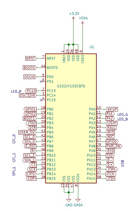
The devices operate from a 2.6V to 3.6V power supply and they are available in –40°C to +85°C temperature range. Several power saving modes provide the flexibility for maximum optimization between wakeup latency and power consumption, which is an essential consideration for designing low power applications.
The above features make the GD32VF103 devices suitable for a wide range of interconnected applications, especially in areas such as industrial control, motor drives, power monitor and alarm systems, consumer and handheld equipment, POS, vehicle GPS, LED display and so on.
Features :
- Flexible memory configurations with up to 128KB on-chip Flash memory and up to 32KB SRAM memory
- Extensive range of enhanced I/Os and peripherals connected to two APB buses
- Wide range of standard and advanced communication interfaces,
- including SPI, I2C, USART and I2S
- Two 12-bit 1Msps ADC with 16 channels, up to four general-purpose 16-bit timers and one PWM advanced timer
- Three power saving modes for maximum optimization between wakeup latency and energy consumption for low-power applications
Its datasheet can be downloaded from the below web link, or by using the QR Code on the right side.
GD32VF103_Datasheet_Rev_1.2.pdf
2.2.3.1 Timing
For the past several decades, quartz-crystal based oscillators, clock generators and resonators were the primary reference timing components in electronics, since there were no real alternatives. Recently a new technology rose up, offering the first devices where the MEMS structures are built in the same package with the analog circuitry. MEMS resonators are connected to the MEMS-specific circuit blocks on the analog IC and are driven through electrostatic excitation. A MEMS bias generator is used to bias the electrostatic transducers that are built in the MEMS die. The resonator sustaining circuit brings the resonator into mechanical oscillation that is sensed, and the analog oscillator die can provide multiple clock outputs from a single, compact semiconductor package.
SiTime, an analog semiconductor company, whose MEMS technology has roots in Bosch and Stanford University, offers solutions that are replacing traditional quartz-crystal based oscillator products by offering higher performance and reliability at a lower cost. SiTime has introduced a combo chip solution that stacks the MEMS structure on top of standard CMOS dice to supply all their timing signals. A key advantage is the ability of the MEMS chip to set up as factory default several clock frequencies on a single chip. The combined MEMS-CMOS solution offers significant benefits such as smaller footprint and less complex chips. Their products are supported by factory programmability and offer drop-in replacements for quartz oscillators without any design changes. The programmable architecture enables flexible product design and fast lead-times, offering in the same time downsizing, with up to 85% space reduction. Designers may also order Time Machine II programmer to program SiTime oscillators in their own facility to quickly develop prototypes. SiTime combined the MEMS and analog electronics on a single die, therefore no need to package the resonator and the analog electronics separately.
Customers can order any combination of frequencies, voltages and frequency stabilities (PPM) in a range of industry-standard packages. SiTime oscillators offer any frequency within the operating range with up to 6 decimal places of accuracy. With custom frequencies, designers can increase system performance (microprocessor / FPGA applications) and reduce bit error rates (Ethernet applications).
Because the devices are made with standard CMOS silicon techniques, they are easier and heaper to manufacture than crystal oscillators, that require special producing and packaging techniques. As the manufacturing process involves fewer participants, the costs are minimized, as well as the time to first sample. Customer benefits not only from the lower price, but also the lower lead-time makes it possible to reduce the investment costs. As MEMS devices offer more features (e.g. programmability), design costs are also less. As reliability is higher, the end product will be of a high brand value.
SiTime's MEMS-based silicon timing product portfolio offers solutions for a wide range of applications. As drop-in replacements for quartz devices, SiTime's oscillators and clock generators are successfully replacing the quartz timing to silicon-based products.
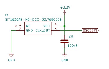
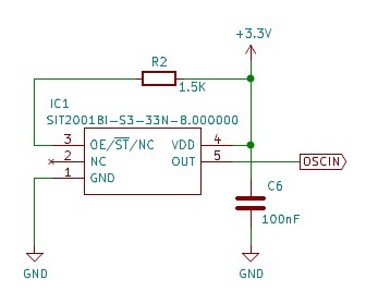
As this new technology definitively has place on IoT applications, we decided to implement 2 different oscillators with MEMS technology on board. The 32 kHz real-time-clock and the 8 MHz oscillator are both from SiTime providing exact heartbeat to the GD32VF microcontroller.
One of the super features of these customizable devices is Programmable Drive Strength. The SiT2001 includes a programmable drive strength feature to provide a simple, flexible tool to optimize the clock rise/fall time for specific applications. Benefits from the programmable drive strength feature are:
- Improves system radiated electromagnetic interference (EMI) by slowing down the clock rise/fall time.
- Improves the downstream clock receiver’s (RX) jitter by decreasing (speeding up) the clock rise/fall time.
- Ability to drive large capacitive loads while maintaining full swing with sharp edge rates.
Further benefits: Silicon is inherently more reliable than quartz. Unlike quartz suppliers, SiTime has in-house MEMS and analog CMOS expertise, which allows SiTime to develop the most reliable products. Unlike quartz, MEMS oscillators have excellent long term aging performance which is why every new SiTime product specifies 10-year aging. SiTime’s oscillators in plastic packages are up to 54 times more immune to external electromagnetic fields than quartz oscillators. High-vibration environments are all around us. All electronics, from handheld devices to enterprise servers and storage systems are subject to vibration. The moving mass of SiTime’s MEMS resonators is up to 3000 times smaller than quartz. SiTime’s oscillators can withstand at least 50,000 g shock. They all maintain their electrical performance in operation during shock events.
Their datasheets can be found here :
You can find further information in the below presentations.
A general comparison of MEMS technology and crystal oscillator technology can be followed here (or scan the QRCode on the rights side):
For using MEMS oscillators in order to save battery lifetime in handheld applications we include here a presentation made on a hands-on training at Endrich. Please follow the below link (or scan the QRCode on the rights side):
2.2.3.2 Powering
The MCU power domain of the Endrich IoT board requires 3.3 V. The power source of the board may be Li battery (3,6V Thionyl-Chloride based ER chemistry primary cells) or USB 5V power coming from either USB charger or rechargeable Li-Ion power-bank. The various input voltage levels and the required low consumption make it necessary to involve - wherever possible - switching mode DC/DC converters. Powering the MCU domain requires step-down conversion, in this case however due to the small currents, it is enough to use LDO ( Low-DropOut) regulators for economic reasons.

2.2.3.3 Controls and signals
LED signals:
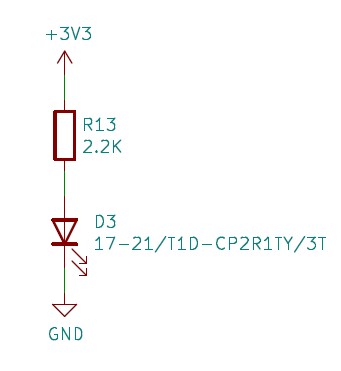
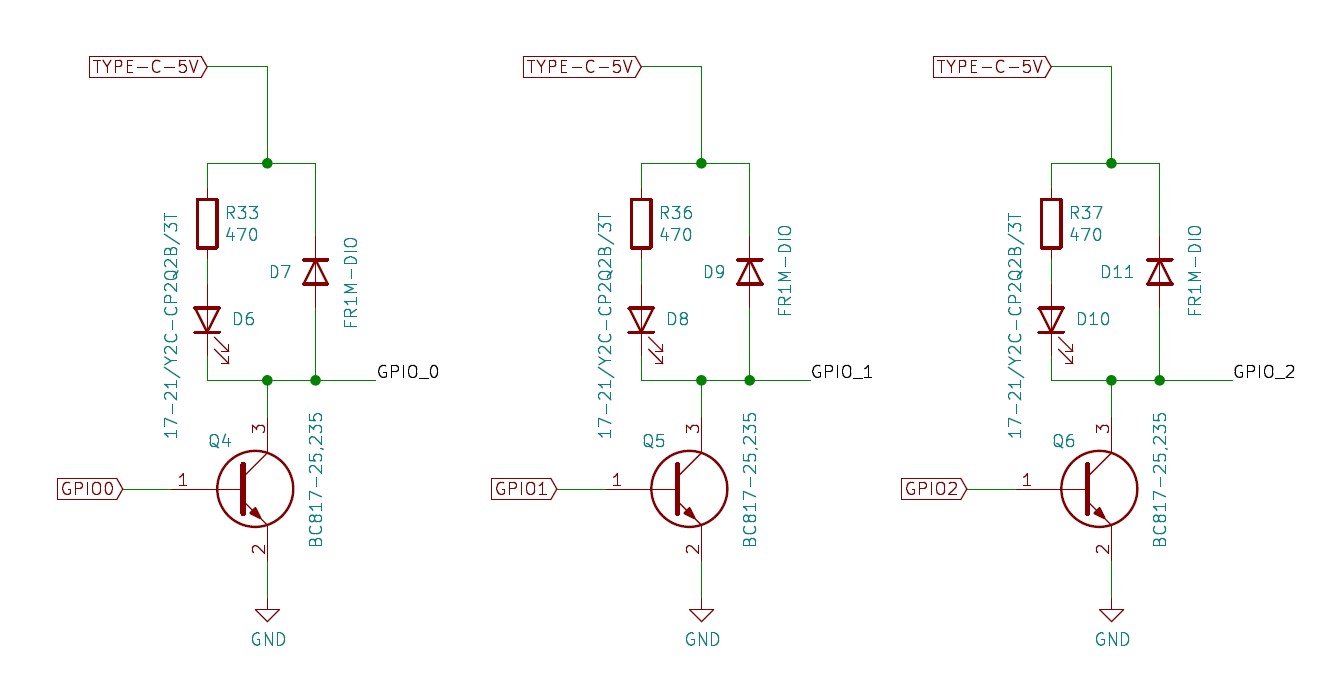
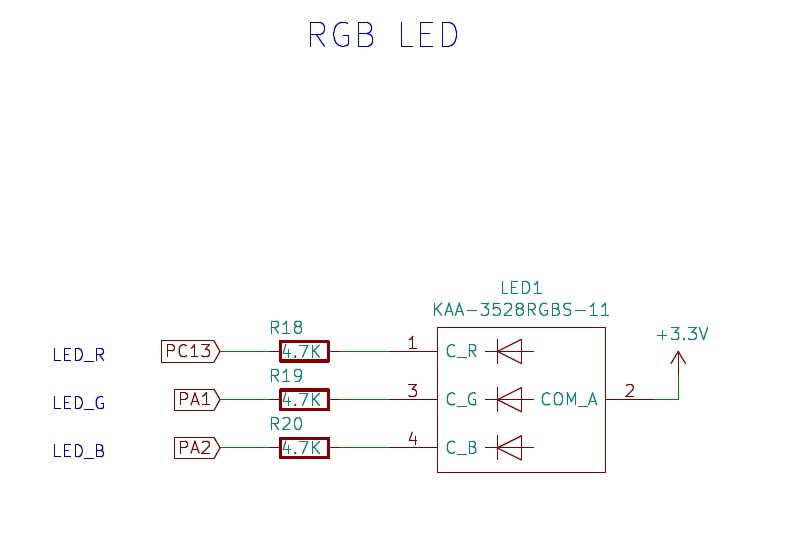
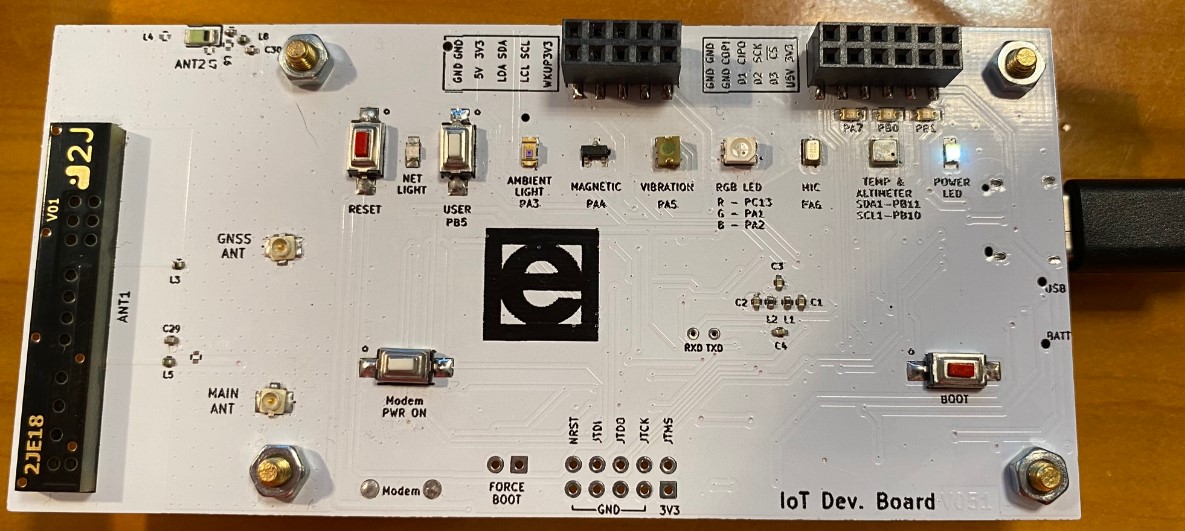
Several LEDs are built in to give visual feedback about operation of the microcontroller. The power ON status LED (D3) is connected to the 3.3V domain output, while there is a 3 color RGB LED (LED1) connected to the PA1, PA2 and PC13 GPIOs to be used for feedbacking user configurable status information. The LEDS (D6, D8, D10) connected to the 3 external GPIOs (PB1, PA7, PB8) show the status (ON/OFF) of the lines.
Control switches and jumpers:
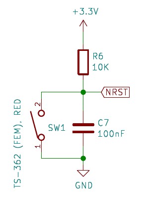
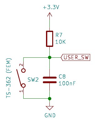
There are several push buttons on board for user interaction. One of them is the RESET button (red) connected to the NRST PIN of the MCU, and also available on J3 Connector’s 10th PIN. The USER switch, which can be used to programmable user function (such as forced sending data, test functions etc.) is connected to the GPIO PB5. The BOOT button (red) connected to BOOT0 PIN of the MCU is for selecting the bootloader mode, and also available on JUMPER J2 3th PIN.
When pressing first BOOT switch and - together with that - the RESET switch ( the two red buttons), the MCU goes to DFU mode ( see 4.2) and the new binary program can be uploaded via the USB interface. Pressing RESET after it, the MCU goes back to normal reset and the update firmware starts to run.
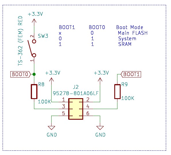
The BOOTLOADER modes can be selected by JUMPERS J2. The choices are boot from main flash, system and SRAM. The J2 BOOT0 pin should be always connected to GND. MCU’s BOOT0 input status will then be selected by SW3 (BOOT). The appropriate selection can be seen in the picture below:
2.2.3.4 Interfaces
The MCU has many external and internal interfaces, which are available for designers. The Endrich IoT SBC Board uses the followings:
- 3 GPIO interfaces to control external devices such as relay boards
- SPI interface to connect external SPI devices such as our own sensor boards or displays
- Standard I2C interface to connect external sensors, and displays
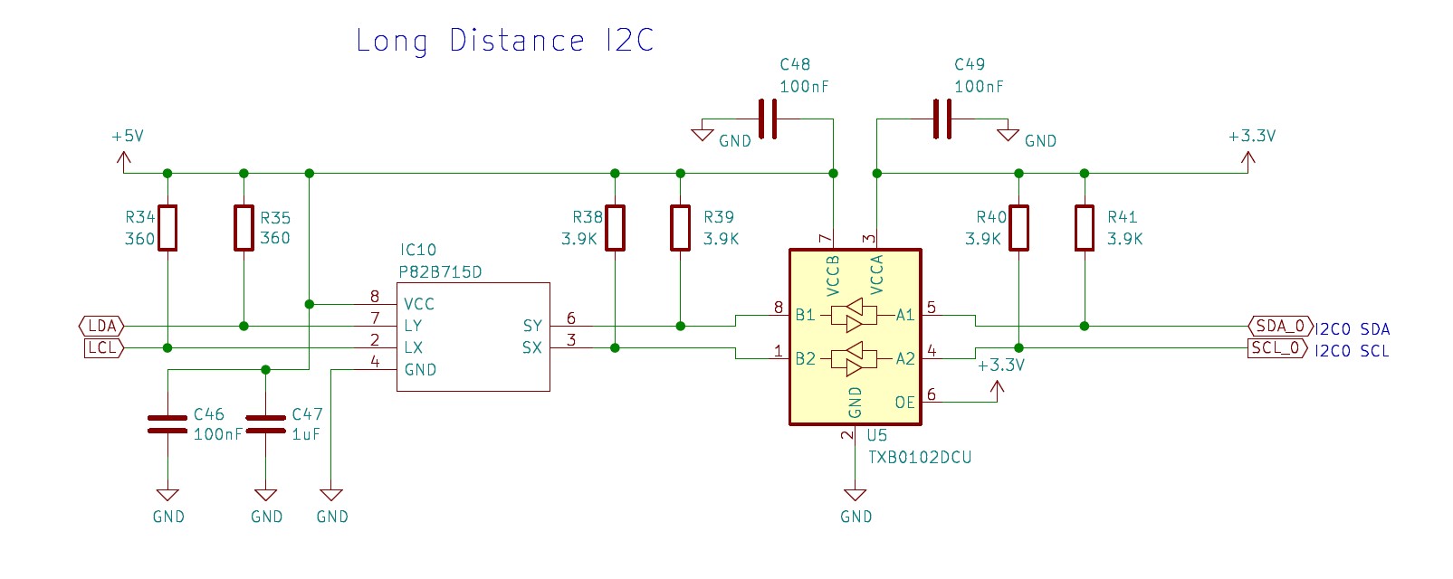
- Long Distance I2C interface to connect our own sensor board with the physical distance up to 50 meters.
- Serial interface (RS232/UART RXT/TXD/DTR) for test purposes
- JTAG/GDLINK for uploading firmware / debugging through special programmer
- USB for accessing the UART of the GD32VF MCU / DFU firmware update
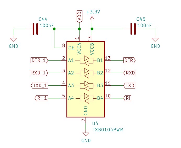
Internal interface: RS232 / UART for interfacing the MA510 GSM modem through level shifter from MCU’s 3.3V TXD/RXD/DTR to GSM Modem’s 3,8V RXD/TXD/DTR lines.
The GPIO interface connectors (J12/8, J12/6, J12/4) are connected to the PA7 , PA8 and PB1 digital outputs of the MCU and offering 0/5V TTL signals to drive external relay boards or other similar devices.

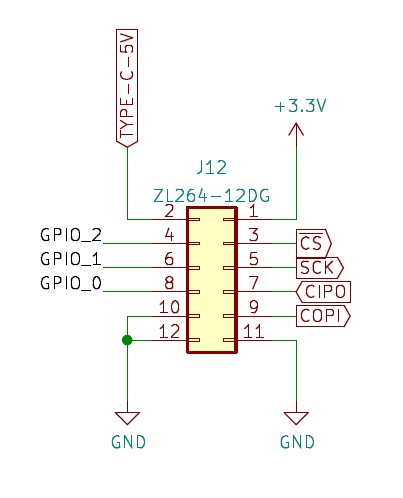
As the GPIOs, the SPI interface is also available on the connector J12. The meaning of the SPI signals are summarized below :
- CS: chip select, activates the communication with a selected peripheral
- SCK: Serial clock
- CIPO: controller In / peripheral Out, receiving when in SPI controller mode, transmitting when in SPI receiver mode
- COPI: controller Out / peripheral In, transmitting when in SPI controller mode, receiving when in SPI receiver mode
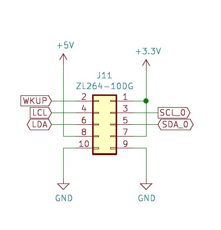
The standard I2C external interface is available on the J11 connector’s 4th and 6th PIN, while the internal I2C interface is used to connect t the onboard Micro Altimeter Sensor module (see 2.2.4.4). As I2C has been defined to be a board level interface, its range is limited and dependent of the bus frequency. In order to extend the distance between controller and peripheral, we have boosted the signal by using amplification. The designed Long Distance I2C interface can be used in connection with Endrich’s I2C Sensor Board up to distance of 50 meters. The connector J11 offers physical connection to both standard and Long Distance I2C interfaces, where LCL/LDA are the clock and data signal of the Long, and SCL and SDA are the clock and data signal of the Standard I2C ports. They are connected to the same output of the MCU (PB6/PB7), so either one or the other channel can be used. The schematics of the solution can be seen below:
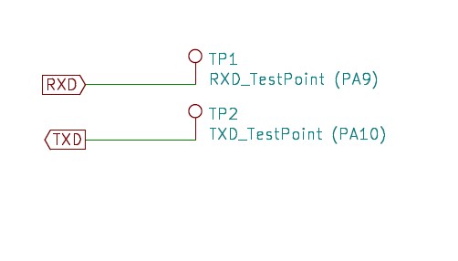
The UART TXD/RXD/DTR signals of the MCU are connected to TP1 and TP2 test-points as well as the input of the level shifter responsible to interface MCU’s 3.3V TXD/RXD/DTR lines to GSM Modem’s 3,8V RXD/TXD/DTR lines.
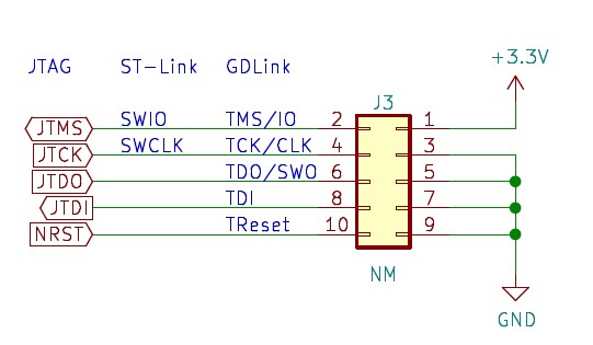
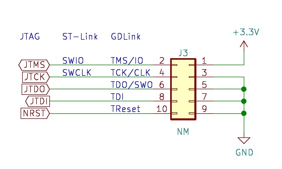
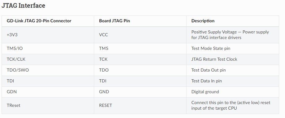
The GD32VF103 MCU can also be programmed from the GD-LINK / JTAG interface by using a GD-Link adapter from GigaDevice. GD-Link adapter is a three-in-one multi-function development tool for GD32 series of MCUs. It provides CMSIS-DAP debugger port with JTAG/SWD interface. User can use GD-Link adapter for online programming or debug code in compatible IDE. Another important function is offline programming. The following figure and table show the electrical connection relationship between GD-Link adapter and JTAG interface of the Endrich IoT SBC Board. We have to connect GD-Link adapter with target board via DuPont lines or other connecting wires.
The USB interface of the board is connected to GD32VF103 MCU’s PA11/PA12 (USB) lines, making possible to access the internal UART as a virtual COM port from external PC as well as to upload binary firmware code to the MCU in DFU mode (see 4.1 and 4.2) by using a DFU device driver on the host PC.
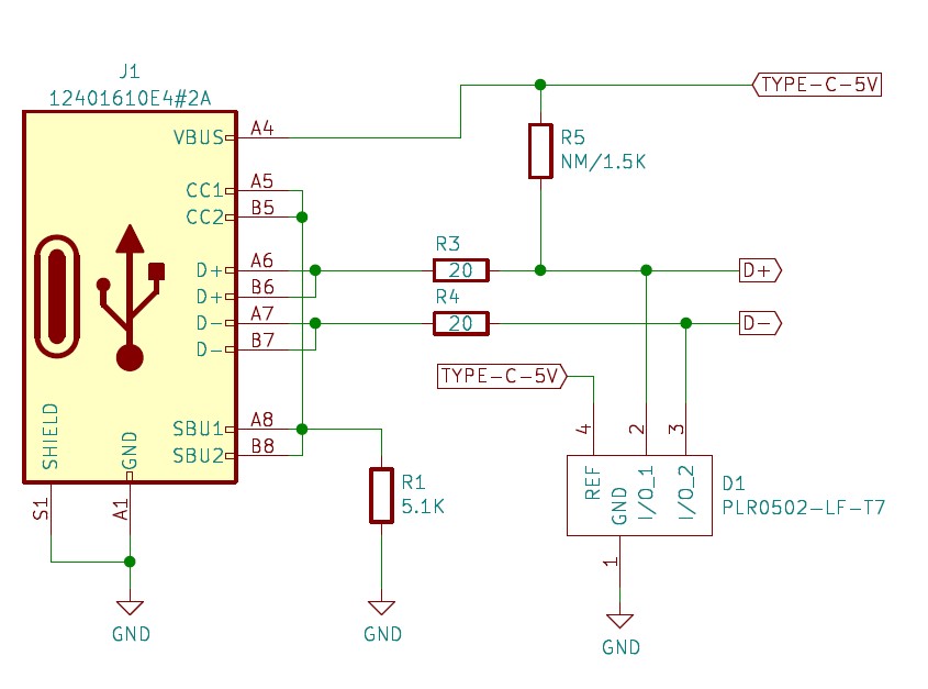
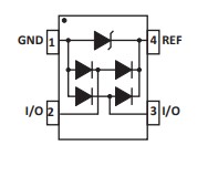
The USB interface of the board is protected against ESD and EFT by using ProTEK Devices’ PLR0502-LF-T7 transient voltage suppressor diode array. The PLR0502 is an ultra low capacitance (0.6pF) steering diode and TVS array combo. This device provides circuit protection for interfaces and wireless bus applications and portable electronics. The PLR0502 is ideally suited to protect USB(1.0-3.0) data I/O ports against the effects of ESD and EFT. The PLR0502 meets the requirements of IEC 61000-4-2 (ESD) and IEC 61000-4-4 (EFT). At higher operating frequencies or faster edge rates, insertion loss and signal integrity are a major concern. The PLR0502 offers a ultra low capacitance and low leakage current in a SOT-543 package.
FEATURES
- Compatible with IEC 61000-4-2 (ESD): Air - 15kV, Contact - 8kV
- Compatible with IEC 61000-4-4 (EFT): 40A - 5/50ns
- 200 Watts Peak Pulse Power per Line (tp = 8/20µs)
- ESD Protection > 25 kilovolts
- Low Clamping Voltage
- Unidirectional Configuration
- Protects 2 I/O Ports and Power Supply
- Ultra Low Capacitance: 0.6pF
- RoHS Compliant
- REACH Compliant
MECHANICAL CHARACTERISTICS
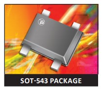
- Molded JEDEC SOT-543 Package
- Approximate Weight: 3 milligrams
- Lead-Free Pure-Tin Plating (Annealed)
- Solder Reflow Temperature: Pure-Tin - Sn, 100: 260-270°C
- 8mm Tape and Reel Per EIA Standard 481
- Flammability Rating UL 94V-0
APPLICATIONS
- Ethernet - 10/100 Base T
- FireWire
- Wireless Communications
- USB 1.0, USB 2.0 & USB 3.0
The datasheet of the device can be accessed in the below link or by scanning the QR code on the right: